We produce several billion high-precision stamped contacts annually for the automotive industry—all of which are manufactured exclusively within the EU. Thanks to their extremely robust design, our press-fit connectors are ideal for high-security applications and wherever maximum mechanical strength is required.
Press-fit Technology: How It Works
Press-fit technology
In the press-fit technique, an electrical connection between the connector and the printed circuit board is established by pressing a connector pin into a through-hole in the board.
The press-fit technique is based on a simple principle: The cross-sectional diagonal of a contact pin’s press-fit zone is larger than that of the metallized PCB hole. The deformation caused during press-fitting is mitigated by the flexible zone on the contact pin. As a result, the PCB sleeve is deformed only to a very small extent. During press-fitting, a cold weld forms between the contact pin and the metallized PCB hole: a gas-tight, corrosion-resistant, low-resistance, and electrically conductive mechanical connection. It remains reliable and stable even under very high mechanical and thermal stresses, such as vibration, bending, and extreme temperature fluctuations.
We recommend process monitoring during the press-fit operation: force-displacement and camera monitoring allow for an assessment of the connection point.
In addition to the proven press-fit technology with our Tcom press® press-fit zone, ept also offers many other connection-technology options. Whether soldered through-hole, THR, or SMT—we have the right solution for every application.
Press-fit technology: Easy to use
Circuit Board Insertion Technology
When the specifications are followed, the press-fit technique is easy to implement. Four parameters play a key role in this process: the drill diameter and the diameter of the metallized press-fit hole, the thickness of the copper sleeve in the press-fit hole, and the surface of the printed circuit board.
If both SMD components and press-fit connectors are to be mounted on a PCB, a specific sequence must be followed: Components with solder terminals must be mounted first. Once all components have been soldered to the PCB using a suitable method, the press-fit connections can be installed. This order is important: Reversing the process sequence would subject the press-fit connections to high thermal stress. This would lead to subsequent (uncontrolled) soldering of the press-fit zone, thereby compromising the integrity of the gas-tight zone.
In addition, the correct distance from the PCB edge and from sensitive electronic components (e.g., ceramic components) as well as the connections of the conductive traces must be observed. Maintaining the minimum distance prevents the PCB material or electronic components from being damaged due to the force exerted by the press-fit zone and the PCB layers from being destroyed.
Press-fit Technology: Advantages
Most robust and reliable bonding technology
Long-lasting durability
Gas-tight bond
High holding forces
No soldering defects, flux residues, or similar issues
No additional cleaning required
Can be recycled by simply squeezing it out
More efficient and cost-effective assembly process
Ideal for PCB coating / potting of the entire assembly
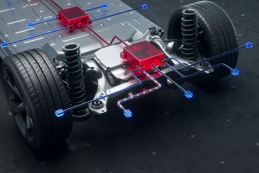
Press-fit Technology: ept's Offering for the Automotive Industry
We manufacture several billion contacts per year, exclusively within the EU, for various sectors and applications in the automotive industry. Our press-fit zones are available in strip thicknesses ranging from 0.2 to 1.2 mm for hole diameters of 0.56 to 2.0 mm, or can be customized to your specifications.
Free white paper on the basics of press-fit technology
Are you looking for in-depth expertise on press-fit technology? For detailed information on the fundamentals of press-fit technology, download our free white paper here.