


White Paper: Fundamentals of Press-Fit Technology
THE PRESS-FIT ZONE AS A ROBUST ALTERNATIVE TO SOLDERING
INTRODUCTION
Since its introduction in the telecommunications sector, press-fit technology has evolved into an established key technology in automotive and industrial electronics. In light of current trends such as electrification, autonomous driving, and Industry 4.0, the demand for reliable and durable connection systems is steadily increasing.
In harsh operating environments involving vibration, temperature fluctuations, humidity, and mechanical stress, the press-fit technique delivers high process reliability and long-term stability. Despite varying press-fit zone designs, all solutions pursue the same goal: a permanently mechanically secure and electrically reliable connection between the printed circuit board and the contact.
This is achieved by designing the press-fit zone larger than the PCB hole and pressing it in with a defined force. This creates a gas-tight, electrically stable, and mechanically robust connection with consistently low contact resistance.
BASICS
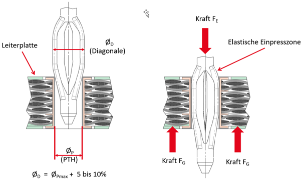
In the press-fit technique, an electrical connection between the connector and the printed circuit board is established by pressing a connector pin into a plated-through hole in the board.
The press-fit technique is based on a simple principle:
the cross-sectional diagonal of the press-fit zone of a contact pin is larger than that of the plated-through hole in the printed circuit board. The deformation caused during insertion is absorbed by the flexible zone on the contact pin, so that the PCB sleeve is only slightly deformed. This creates a cold weld between the contact pin and the plated-through PCB hole: a gas-tight, corrosion-resistant, low-resistance, and highly electrically conductive connection. This connection remains permanently stable even under high mechanical and thermal stresses—such as vibration, bending, and extreme temperature fluctuations.
We recommend process monitoring during the insertion process. Force-displacement analyses and camera-based systems enable a reliable assessment of the connection quality.
In addition to the proven insertion technology with our Tcom press® insertion zone, ept also offers other connection technologies, such as soldered through-holes, THR, or SMT—each tailored to the specific application.
ADVANTAGES OF PRESS-FIT TECHNOLOGY
Compared to conventional soldering, press-fit technology offers numerous advantages in terms of quality, cost-effectiveness, functionality, and environmental impact. It is characterized by very high reliability and mechanical strength and is particularly resistant to shock and vibration. In addition, it prevents common defects such as cold solder joints or short circuits.
Press-fit technology also offers compelling economic benefits due to its reparability and cost-effective assembly. Functionally, it enables reliable processing without thermal stress on the printed circuit board, thereby protecting components. At the same time, connector contacts remain free of solder.
Furthermore, press-fit technology offers environmental benefits, as it produces neither solder fumes nor flux residues and eliminates the need for additional cleaning processes. It thus complies with current environmental requirements and directives such as RoHS and WEEE.
DRAWBACK OF THE PRESS-FIT TECHNIQUE
Despite its many advantages, the press-fit technique also has some limitations compared to soldering. It places high demands on PCB quality, particularly regarding hole diameters and tolerances, and requires specialized tools and equipment, which leads to higher investment costs.
In addition, the press-fit process generates mechanical stresses that can cause damage if not applied properly. Miniaturization is also somewhat limited compared to soldering technology.
In addition, the press-fit process generates mechanical stresses that can cause damage if not applied properly. Miniaturization is also somewhat limited compared to soldering technology.
SELECTION CRITERIA FOR PRESS-FIT TECHNOLOGY
A reliable press-fit connection depends on the optimal interaction of several quality characteristics. Key factors include the design of the press-fit zone, the specific application, the properties of the printed circuit board, and the manufacturing process.
Only when these factors are properly coordinated can press-fit technology achieve its full potential and ensure a connection that is durable, mechanically robust, and electrically safe.
Only when these factors are properly coordinated can press-fit technology achieve its full potential and ensure a connection that is durable, mechanically robust, and electrically safe.
I. Selection Criteria for Printed Circuit Boards
The table compares different PCB surface finishes in terms of layer thickness and suitability for the press-fit technique.
| Surface | |||||
| Immersion Sn | ENIG | Immersion Ag | OSP | Lead-free HAL | |
| Coating thickness | 0.8 to 0.2 µm | 5 µm Ni 0.1 µm Au | 0.1–0.2 µm | 0.1–0.5 µm | 5–50 µm |
| Suitability for press-fit technology | very good | limited* | limited* | good | limited* |
Immersion tin is the most suitable option; OSP is rated as good, while ENIG, immersion silver, and lead-free HAL are only suitable to a limited extent—depending on the application.
In addition, typical plating zones are shown, which usually consist of tin or tin alloys on a nickel layer. Overall, the brochure makes it clear that the choice of surface has a decisive influence on the quality and reliability of the press-fit technology and must be carefully selected depending on the application.
In addition, typical plating zones are shown, which usually consist of tin or tin alloys on a nickel layer. Overall, the brochure makes it clear that the choice of surface has a decisive influence on the quality and reliability of the press-fit technology and must be carefully selected depending on the application.
II. Selection Criteria for the Press-Fit Zone
The following surface finishes are available in the plating zone: matte tin, tin-lead, silver-tin, tin-silver, and indium coatings, each applied over a nickel layer.
| Surfaces | ||
| 0.30–1.50 µm Sn matte | over | 1–3 µm Ni matte |
| 0.30–1.50 µm SnPb 92/8–97/3 matte | over | 1–3 µm Ni matte |
| 0.35–1.50 µm AgSn or SnAg | over | 1–3 µm Ni matte |
| 0.30–1.50 µm In | over | 1–3 µm matte Ni |
The right surface finish is critical for a reliable press-fit connection. It affects the press-fit forces and must be able to deform plastically under load without being damaged. At the same time, it ensures a stable electrical contact, protects against corrosion, and reduces contact resistance. A suitable coating also helps prevent damage to the printed circuit board and ensures a safe, repeatable process.
HOLE CONSTRUCTION
To ensure a high-quality press-fit connection, special attention must be paid to the drill hole diameter, the finished hole diameter, the copper sleeve thickness, and the PCB surface during PCB manufacturing.
The correct hole structure is crucial, as it directly influences the mechanical stability and electrical reliability of the connection. Only with correctly matched hole and sleeve dimensions is the necessary press fit achieved, which ensures a secure hold and consistent contact. Deviations can lead to excessive press-fit forces, damage to the through-hole plating, or insufficient contact. In addition, a suitable hole design helps to compensate for manufacturing tolerances and ensure consistent process quality.
The following hole design represents an exemplary implementation.
| LP material | FR4 | |
| Nominal hole | Ø 1.0 mm | |
| A | PCB thickness | min. 1.44 mm |
| B | End hole | Ø 1.0 +0.09 / -0.06 mm |
| C | Base hole | 1.15 ±0.025 mm |
| D | Cu layer | min. 25 µm |
| E | Surface | Chemical Sn layer, 0.5–1.5 µm |
| F | Residual ring | min. 0.1 mm |
PROCESSING
A controlled insertion process is crucial for a connection that remains mechanically and electrically reliable over time. The use of an upper tool and a counterholder is absolutely essential.
The upper tool transfers the force of the press to the contact, while the counterholder supports the printed circuit board and protects it from mechanical stress. Depending on the connector, flat-plate or comb tools are used.
If the tools are not optimally matched, undesirable forces can act on the PCB and damage components that have already been mounted. The insertion force should be fully absorbed by the lower tool.
PCBs with inserted connectors should not be heated above 125 °C.

Conclusion
Press-fit technology represents a high-performance and future-proof alternative to traditional soldering. It offers high process reliability, excellent mechanical stability, and a permanently reliable electrical connection—even under demanding operating conditions.
Especially in light of increasing electrification, rising power densities, and growing demands for robustness and service life, press-fit technology offers decisive advantages. However, optimal performance requires precise interaction between the press-fit zone, the printed circuit board, and the manufacturing process.
A key success factor is the selection of an optimally designed press-fit zone. The press-fit zones from ept GmbH—particularly the Tcom press® technology—are characterized by highly controllable press-fit behavior, low stress on the printed circuit board, and high process window stability. This minimizes damage to the through-hole plating while ensuring permanently stable electrical contacts. Furthermore, the geometry of the ept press-fit zone enables reliable processing even with tight tolerances and complex PCB structures.
As an experienced specialist in connection technology, ept GmbH offers customized solutions for all aspects of press-fit technology. With innovative technologies such as the Tcom press® press-fit zone, comprehensive application expertise, and high manufacturing competence, ept supports its customers in implementing reliable and cost-effective connection solutions for demanding applications.