


White Paper: Board-to-Board Connectors for Industrial Sensors and Camera Systems
Faster, smaller, more robust: When used in industrial sensors and camera systems, connectors must meet an ever-increasing number of requirements. The trend is toward modularization. With the help of board-to-board connectors, printed circuit boards can be flexibly combined with one another, thereby significantly determining the sensor’s functionality. In the age of Industry 4.0, connectors must not only become smaller and more powerful—in addition to miniaturization and high speed, use in industrial environments often requires extreme ruggedness. This guide is designed to help you find the right connector for your machine vision application.
Three key requirements are central to the development of modern sensors and camera systems for industrial applications: high-speed data transmission, miniaturization, and ruggedness. These requirements can rarely be considered in isolation from one another—however, depending on your priorities, you can find the optimal connector for your application.
High-speed data transfer
In the age of big data, IoT, and IIoT, smart sensors and cameras in industrial environments also require secure, high-speed data transmission. Connectors for high-speed applications should feature a correspondingly high-performance contact design. Since a connector’s geometry inherently poses a certain risk of fluctuations in impedance, special attention must be paid during the development of high-speed connectors to optimizing the contact design for impedance control. In this context, it is important to minimize cross-sectional changes within the connector as much as possible, as these result in impedance fluctuations, which in turn lead to losses in signal transmission.
In the case of miniaturized assemblies, connectors should also feature electromagnetic shielding, as high-frequency signals in particular are highly susceptible to unwanted electromagnetic effects. Even a small pulse can be enough to distort the useful signal, preventing the receiver from unambiguously interpreting the digital states.
A connector can act as both an interference sink and an interference source; that is, it can be subject to interference from other components in the assembly while also exerting its own electromagnetic influence on surrounding components. The coupling inductance LK, measured in picohenries (pH), allows the connector to be characterized in both roles—source and sink. A simple test setup helps users determine which connector and which pinout is necessary or optimal for their specific application. To do this, the useful signal must be disturbed using a burst generator, and the maximum permissible coupling inductance must be measured. If the induced voltage (Uind), the generator voltage (UGen), and the generator constant (kGen) are known, the specific, maximum permissible coupling inductance (L) for each application can be determined using the following formula:
L = Uind / (UGen * kGen)
The coupling inductance also helps the user define the appropriate connector in terms of its electromagnetic compatibility. This allows for the avoidance of costly and time-consuming trial-and-error testing in the EMC laboratory.
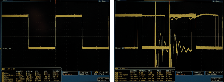
It is also possible to reduce the coupling inductance of a connector using shielding. Here is an application example: For an HDMI signal, a case-specific maximum coupling inductance of 47 pH was determined at a voltage of 4.4 kV. If the value exceeds this, the signal can no longer be transmitted without interference. The following figure shows that the coupling inductance was significantly reduced through the use of a shielding concept.
A connector can act as both an interference sink and an interference source; that is, it can be subject to interference from other components in the assembly while also exerting its own electromagnetic influence on surrounding components. The coupling inductance LK, measured in picohenries (pH), allows the connector to be characterized in both roles—source and sink. A simple test setup helps users determine which connector and which pinout is necessary or optimal for their specific application. To do this, the useful signal must be disturbed using a burst generator, and the maximum permissible coupling inductance must be measured. If the induced voltage (Uind), the generator voltage (UGen), and the generator constant (kGen) are known, the specific, maximum permissible coupling inductance (L) for each application can be determined using the following formula:
L = Uind / (UGen * kGen)
The coupling inductance also helps the user define the appropriate connector in terms of its electromagnetic compatibility. This allows for the avoidance of costly and time-consuming trial-and-error testing in the EMC laboratory.
It is also possible to reduce the coupling inductance of a connector using shielding. Here is an application example: For an HDMI signal, a case-specific maximum coupling inductance of 47 pH was determined at a voltage of 4.4 kV. If the value exceeds this, the signal can no longer be transmitted without interference. The following figure shows that the coupling inductance was significantly reduced through the use of a shielding concept.

In this test, the boardlocks and the outer contacts were connected to ground potential for both the unshielded and shielded versions, while a signal was applied via a pair of contacts. The measured coupling inductance values can be demonstrated using color-coded maps of the electric and magnetic fields. The simulation with an unshielded connector showed that a coupling inductance of up to 196 pH is present in this case. Given the determined threshold value of 47 pH, undisturbed signal transmission would no longer be guaranteed. With the shielded connector, however, the coupling inductance values range from 1 to 4 pH. These were thus reduced by a factor of approximately 50 due to the shielding, thereby ensuring interference-free transmission. With a higher number of poles, a reduction by a factor of 100 to 200 is even possible.
For the user, the shielding offers two key benefits: First, the connector acts as a reduced source of interference; second, the shielding makes it a lower sink for interference signals. By using shielded connectors, they can now also be positioned closer to sources and sinks of interference on the printed circuit board. Additionally, this enables a higher performance class in the required burst and surge tests of the electrical device.
For the user, the shielding offers two key benefits: First, the connector acts as a reduced source of interference; second, the shielding makes it a lower sink for interference signals. By using shielded connectors, they can now also be positioned closer to sources and sinks of interference on the printed circuit board. Additionally, this enables a higher performance class in the required burst and surge tests of the electrical device.
miniaturization
Despite increasing functional integration, the size of sensors and camera systems must not increase. In most cases, industrial automation actually demands continuous miniaturization to enable the construction of ever-more-compact machines. Similarly, the trend toward modular sensor and camera designs requires the use of correspondingly miniaturized connectors. Over the past decades, connectors have therefore been reduced to a fraction of their original size while maintaining nearly identical performance.

Surface-mount technology is ideal for applications with particularly limited space. It is especially space-efficient because it allows for double-sided PCB assembly and small pitch. With insertion technology, for example, a tight pitch of just 0.5 mm would not be feasible due to the physical forces acting during the insertion process—nor would double-sided PCB assembly. In miniaturized applications, another crucial selection criterion for the appropriate connector is the spacing of sensitive components within the assembly: these are often positioned very close together, increasing the risk of mutual electromagnetic interference. To ensure reliable data transmission, electromagnetic compatibility (EMC) protection is therefore becoming increasingly important. To avoid signal interference, it is recommended—as with high-speed connectors—to select a shielded connector here as well.
Robustness
Sensors and camera systems used in close proximity to machinery are particularly exposed to harsh environmental conditions. To protect the electronics from these external influences, the entire assembly can be potted. However, this requires a connection solution that is also compatible with potting. Conventional connectors are clearly at a disadvantage here because the vulnerable mating area must be protected from the potting compound. The spring-blade contact technology used here would not provide the necessary IP protection rating for these materials.

When selecting the appropriate connector, it is therefore important to choose a one-piece connection solution—that is, a connector that does not require a conventional mating area. This allows the potting compound to provide a durable and robust connection while preventing it from penetrating the contact area.
If electronic components need to be tested for robustness, this can be done through laboratory testing. In these tests, the standardized shock profile must correspond to the target condition, i.e., an acceleration of 50 g with a tolerance of 20 percent (high abort and low abort). According to DIN EN 60068-2-27, a contact interruption of ≤ 1 µs is permissible.
If electronic components need to be tested for robustness, this can be done through laboratory testing. In these tests, the standardized shock profile must correspond to the target condition, i.e., an acceleration of 50 g with a tolerance of 20 percent (high abort and low abort). According to DIN EN 60068-2-27, a contact interruption of ≤ 1 µs is permissible.

If the connector in your application is exposed to extreme external environmental influences such as vibration, shock, moisture, dirt, extreme temperatures, or temperature fluctuations, extreme ruggedness is required. Encapsulating your assembly can help, but it is advisable not to rely solely on this method. Instead, a combination of encapsulation and press-fit technology is recommended. This method has already proven itself billions of times over and is considered the most robust and reliable connection option—even under adverse conditions. In press-fit technology, the connector pin is pressed into a through-hole in the PCB, thereby creating both an electrical and mechanical connection between the connector and the PCB. At the same time, this can result in cost savings of up to 50 percent, as it eliminates the need for labor-intensive soldering and expensive cable solutions. Without the vulnerable plug area, a connector using the press-fit technique can even withstand shock loads of 50 to 200 g without contact interruption.
When all-rounders are in demand
In theory, these requirements—high-speed data transmission, miniaturization, and ruggedness—can be considered in relative isolation from one another. As a user, however, you will likely find that the connector you need rarely has to meet just one of these requirements. For this reason, many connectors meet several of these criteria to varying degrees. In some cases, it’s also worth taking a look at the “all-rounders” among connectors. When multiple connectors are required simultaneously, selecting a scalable product family streamlines procurement and ensures compatibility across all variants—shielded, unshielded, straight, or angled—while avoiding time-consuming and costly approval cycles.

Any questions?
As experts in PCB connectors and contact technology, we share our expertise through webinars tailored to your requirements:
www.webinar.ept-group.de.
Please contact us directly for any technical inquiries regarding connectors.
ept GmbH
Bergwerkstr. 50
86971 Peiting, GERMANY
Phone +49 (0) 88 61 2501-0
Fax +49 (0) 88 61 2501-700
www.ept.de sales@ept.de
www.webinar.ept-group.de.
Please contact us directly for any technical inquiries regarding connectors.
ept GmbH
Bergwerkstr. 50
86971 Peiting, GERMANY
Phone +49 (0) 88 61 2501-0
Fax +49 (0) 88 61 2501-700
www.ept.de sales@ept.de