


- back
- Description
- Technical Specifications
- Hole Specifications
- Modifications
- Packaging
- Downloads
- Stock Check
flexilink b-t-b, 15 mm height Part No. 990-52XNN150-110
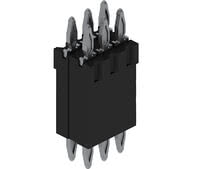
Illustration similar
Parallel
Press-fit
Power
Rugged
- 15 mm height
- for two-stage press-in operation
- 1 - 3 contact rows
- space & cost saving
- part number key: X = number of rows, NN = contacts per row
- For requests please contact our sales department.
Technical Specifications
Basics
| No. of Contacts | 2 - 90 (max. 30 per row) |
|---|---|
| Termination Technology | Press-fit |
| Board-to-Board Distance | 15 mm |
| Operating Temperature Range | -40°C to +125°C |
Material
| Insulator Material | PBT |
|---|---|
| CTI value IEC 60112 | 250 |
| Contact Material | Copper alloy |
| Plating | Sn |
Mechanical
| Pitch | 2.54 mm or individually assembled |
|---|
Electrical
| Operational Current | max. 11 A at 20°C per pin (1x10 pins, height 15 mm) max. 7 A at 20°C per pin (2x10 pins, height 15 mm) max. 6 A at 20°C per pin (3x10 pins, height 15 mm) |
|---|---|
| Contact Resistance | <5 mΩ |
| Clearance and Creepage | min. 0.44 mm / 0.57 mm (within the row) min. 1.94 / 2.07 mm (between the rows) |
Processing
| Assembly | manual / semi-automatic / fully automatic |
|---|
Approval / Compliance
| UL file | E130314 |
|---|---|
| Environment | RoHS compliant |
Hole Specifications

| Material | imm. Sn printed circuit boards |
|---|---|
| Nominal Hole | Ø 1.0 mm |
| A PCB Thickness | min 1.4 mm |
| B Plated Hole | Ø 1.0 +0.09 / -0.06 mm |
| C Drill Hole | 1.15 ±0.025 mm |
| D Cu Plating | min. 25 µm |
| E Surface | imm. Sn plating, max. 1.5 µm |
| F Annular Ring | min. 0.1 mm |
| Material | Ni, Au printed circuit boards |
|---|---|
| Nominal Hole | Ø 1.0 mm |
| A PCB Thickness | min 1.4 mm |
| B Plated Hole | Ø 1.0 +0.09 / -0.06 mm |
| C Drill Hole | 1.15 ±0.025 mm |
| D Cu Plating | min. 25 µm |
| E Surface | Ni, Au plating, 0.05 - 0.2 µm Au over 2.5 - 5 µm Ni |
| F Annular Ring | min. 0.1 mm |
| Material | pure Cu printed circuit boards |
|---|---|
| Nominal Hole | Ø 1.0 mm |
| A PCB Thickness | min 1.4 mm |
| B Plated Hole | Ø 1.0 +0.09 / -0.06 mm |
| C Drill Hole | 1.15 ±0.025 mm |
| D Cu Plating | min. 25 µm |
| E Surface | OSP, z.B. GLICOAT-SMD (F2) with 0.12 - 0.15 µm |
| F Annular Ring | min. 0.1 mm |
Plated through-hole according to IEC 60352-5
Modifications
Available on request
- other pin configurations
Packaging
Bulk or Tray