


Press-fit technology for connectors
Press-fit technology: How it works
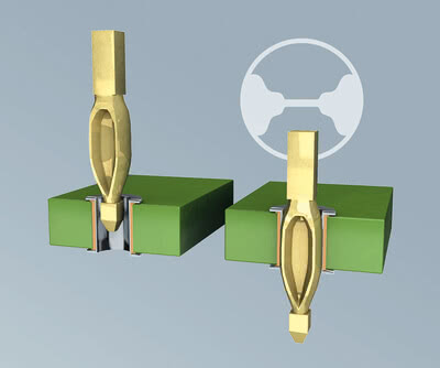
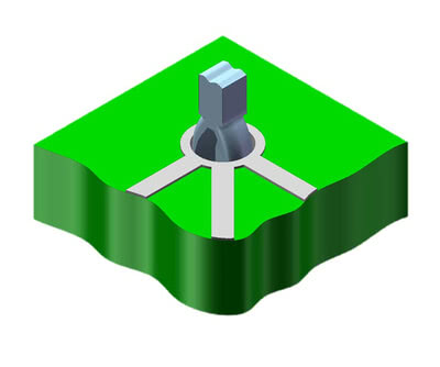
With press-fit technology, an electrical connection is created between the connector and the PCB by pressing a connector pin into a plated-through PCB hole.
The press-fit technique is based on a simple principle:
The press-fit zone of a contact pin has a larger diagonal cross-section than the metallized PCB hole. The deformation that occurs during press-fitting is reduced by the flexible zone on the contact pin. The PCB sleeve is therefore only deformed to a very small extent. During the press-fit process, a cold weld is created between the contact pin and the metallized PCB hole: a gas-tight, corrosion-resistant, low-resistance and electrically conductive mechanical connection. It remains contact-safe and stable even under very high mechanical and thermal loads, such as vibration, bending and strong temperature changes.
We recommend in-process monitoring during the press-fit process: force-displacement and camera monitoring allow the connection point to be assessed.
In addition to the proven press-fit technology with our Tcom press® press-fit zone, ept also offers many other connection technology options. Whether soldered through-hole plating, THR or SMT - we have the right solution for every application.
Press-fit technology: What you need to know
The press-fit technology is easy to handle if the specification is adhered to. Four parameters play a key role here:
The drill diameter and the diameter of the metallized press-fit hole, the thickness of the copper sleeve in the press-fit hole and the PCB surface.
If both SMD components and press-fit connectors are to be accommodated on a PCB, a certain sequence must be observed:
The components with solder connections must be mounted first. Once all components have been soldered onto the PCB using a suitable process, the press-fit connectors can be mounted. This sequence is important: reversing the process sequence would result in a high thermal load on the press-fit connections. This would lead to subsequent (uncontrolled) soldering of the press-fit zone, which would no longer guarantee an intact gas-tight zone.
In addition, the correct distance to the edge of the PCB and to sensitive electronic components (e.g. ceramic components) as well as the connections of the conductor tracks must be observed. Maintaining the minimum distance prevents the PCB material or electronic components from being damaged by the force of the press-fit zone and the PCB layers from being destroyed.
Press-fit technology: Advantages
- Most robust and reliable connection technology
- Long-lasting durability
- Gas-tight connection
- High holding forces
- No soldering defects, flux residue or similar
- No additional cleaning necessary
- Recycling possible by simply pressing out
- Efficient and cost-effective assembly process
Press-fit technology: ept's offer for the automotive industry
We manufacture several billion contacts per year for various sectors and applications in the automotive industry. Our press-fit zones consist of strip thicknesses of 0.2 to 1.2 mm for hole diameters of 0.56 to 2.0 mm or according to your requirements.
Free whitepaper on the basics of press-fit technology
Are you looking for detailed specialist knowledge about press-fit technology?
For detailed information on the basics of press-fit technology, we will be happy to send you our free white paper:
Request whitepaper "
For detailed information on the basics of press-fit technology, we will be happy to send you our free white paper:
Request whitepaper "
Press-fit technology: Application
Due to their extremely robust properties, the press-fit connectors are used for high-security applications or where high mechanical robustness is required.